


Review of fundamentals
In order to understand the effects of PCB parasitic inductances and capacitances, it may be useful to review some fundamental concepts.
Inductance
Estimating the inductance of a PCB track is very difficult and made even more so given the high frequency effects on current flow such as eddy currents and skin effect. However, a review of a fundamental formula for inductance shows how it can be minimised.
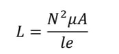
where N = number of turns, μ = permeability, le = magnetic path length, A = cross section area
For an electronic circuit, the number of turns, N, is normally equal to one; that is the go and return path of the current in question. The cross-section area, A, is the area encompassed by this current and is one parameter we can control through good PCB layout practices.
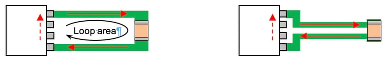
Figure 1: Reducing cross sectional loop area reduces inductance
Capacitance
As with the inductance of PCB tracks, calculating the capacitance between two areas of PCB copper is very difficult. Again, looking at a fundamental formula for the capacitance between two conductors can show what parameters we can control with the PCB design.
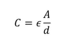
where ε = permittivity, A = common area of the plates, d = distance between the plates
The permittivity is a function of the PCB material; normally FR4 with a permittivity of 4.7. ‘d’ is the distance between the overlapping copper as is defined by the PCB stack up. ‘A’ is the common area or area of overlap of the conductors.
It is normal practice to use wide and large areas of copper, such as ground planes, to reduce trace impedance. However, it should be remembered that such large areas can add significant capacitance to a sensitive circuit node and the effect of this capacitance must be borne in mind.
Vias
Again, calculating the inductance of a PCB via is very difficult. A good rule of thumb is 1nH per via. This needs to be borne in mind when deciding if it is better to use vias to an internal layer or keep the go and returns traces on the same layer.
Voltage and current formulae
Looking at the fundamental formulae for voltages and currents in capacitors and inductances, it can be seen that a critical factor is the ‘rate of change’ of the voltage or current rather than the amplitude of the changing voltage or current itself.
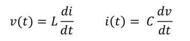
That is, in the case of an inductor, a rapidly changing current, even if that current is small in amplitude, can result in a large voltage drop across the inductor (or PCB trace). A current of 10mA switching in 1ns will result in the same voltage drop as a current of 10A switching in 1µs.
Similarly, for capacitors, a rapidly changing voltage across the capacitor can result in a very large current. This current must always return to its source and if not managed correctly with good PCB layout can result in unwanted EMI interference.
With power converter circuits, the trend towards higher powers and higher switching frequencies can mean switching 10s or 100s of volts or amps with rise and fall times of sub 10ns. With these levels of switching speeds, every nano-henry or pico-farad can have a significant effect on circuit performance.
Gate driver circuit
The HEY1011 is a driver module for driving GaN FETs, https://www.heyday-ic.com/gan-drivers. The HEY2011 driver range are excellent for driving MOS FET switches, https://www.heyday-ic.com/mos-drivers.
Heyday drivers have the unique advantage in that they require the minimum of external components, particularly on the output side, which is the most critical from a PCB layout point of view. The Heyday drivers do not require a separate isolated or bootstrap diode – all of that functionality is included in the drivers using our unique Power-thru® technology.
The pinout of the device has been carefully designed for ease of PCB layout and optimum performance.
Good quality decoupling capacitors should be used for decoupling the primary, VDRV, and secondary, CSEC, voltages. And again, the HEY1011 LGA pinout has been designed for the optimimum positioning of these capacitors.
The OUTPU (FET drive on) and OUTPD (FET drive off) can be used directly to the FET gate or with series resistors to control the FET rise and fall times. Having these functions separated but adjacent on the module allows for independent control of the turn on and off times without the need for external parallel diode or transistors circuits while still allowing the driver to be as close as possible to the driven FET.
The gate drive current return to the module is through the OUTSS pins and these have been positioned to allow for the minimum loop area for the gate current.
The example PCB layout below shows the HEY1011 used with a GaN Systems GS66516T FET and follows the recommended layout for the GS66516T and the principles described above.

Figure 2 : HEY1011 PCB layout with GaN Systems GS66516T