


APEK85110-KNH-01
HALF BRIDGE DRIVER SWITCH BOARD with AHV85110 gate driver
Content
Description - Quick Start Guide - Gate pull up and pull down resistors - PCB Layout - Schematic - Bill of materials - Double Pulse Test - Test results - Ordering Information - Disclaimer -
Description
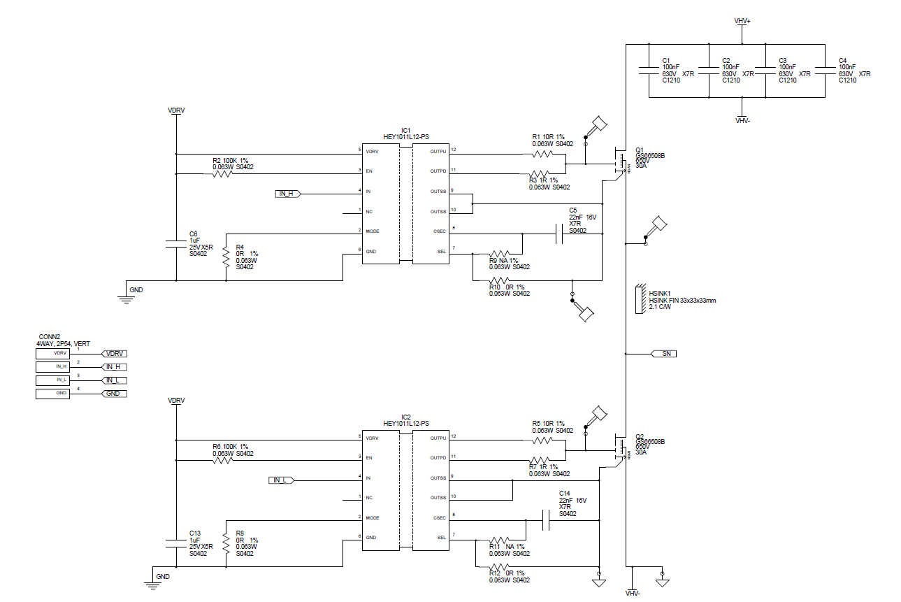
The Heyday Integrated Circuits Half Bridge Driver-Switch HEY-HBDS-G-12A1-A board is a demonstration board containing two HEY1011-L12A GaN FET drivers and two GaN FETs configured in a half bridge configuration.
The datasheet for the HEY1011 in this board can be found in our resources
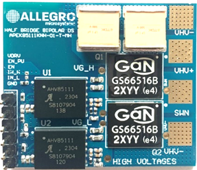
Figure 1: Allegro APEK85110KNH-01 Evaluation Board
The APEK85110KNH-01 can be used to perform double pulse tests, see section Double Pulse Test below, or to interface the half bridge to an existing LC power section as shown below.
The isolated APEK85110KNH-01 driver does not require secondary side power nor bootstrap components. Gate drive power is supplied to secondary side from the primary side supply voltage VDRV. The amplitude of the gate drive can be varied by varying VDRV between 7V and 15V.
The Allegro Microsystems Half Bridge Driver-Switch is available in two versions:
-
APEK-HBDS-G-12A1-A Top Cooled: Uses GaN Systems GS66516T devices mounted on the bottom side of the PCB where a heat sink, if used, can be mounted direct onto the transistors
-
APEK-HBDS-G-12B1-A Bottom Cooled: Uses GaN Systems GS66508B devices mounted on the top side of the PCB where a heat sink, if used, can be mounted on the bottom side of the PCB and heat is transferred through the PCB.
|
|
DANGER DO NOT TOUCH THE BOARD WHEN IT IS ENERGIZED AND ALLOW ALL COMPONENTS TO DISCHARGE COMPLETELY PRIOR HANDLING THE BOARD. HIGH VOLTAGE CAN BE EXPOSED ON THE BOARD WHEN IT IS CONNECTED TO POWER SOURCE. EVEN BRIEF CONTACT DURING OPERATION MAY RESULT IN SEVERE INJURY OR DEATH. Please ensure that appropriate safety procedures are followed. This evaluation kit is designed for engineering evaluation in a controlled lab environment and should be handled by qualified personnel ONLY. Never leave the board operating unattended. |

|
WARNING Some components can be hot during and after operation. There is NO built-in electrical or thermal protection on this evaluation kit. The operating voltage, current, and component temperature should be monitored closely during operation to prevent device damage. |

|
CAUTION This product contains parts that are susceptible to damage by electrostatic discharge (ESD). Always follow ESD prevention procedures when handling the product. |

Quick Start Guide
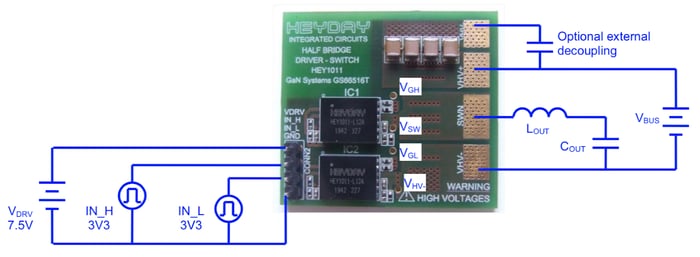
Figure 2: HEY-HBDS-G-12A1-A Quick Start
-
Apply VDRV = 7.5V
-
Apply input gate signals, with adequate dead time, to the IN_L and IN_H inputs.
-
Convenient test points a located on the test board as shown above. A suitable differential oscilloscope should be used to monitor the high side gate signal from VGH to VSW.
PCB Layout
HEY-HBDS-G-12A-A
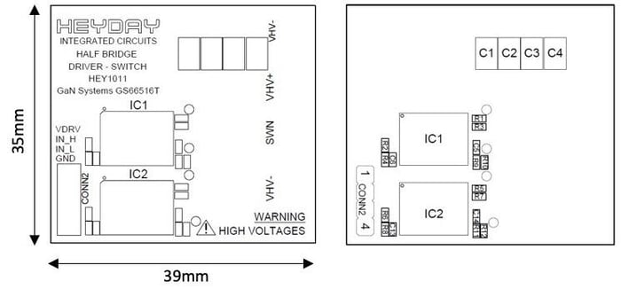
Figure 3: HEY-HBDS-G-12A1-A Silkscreen and component placement
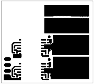
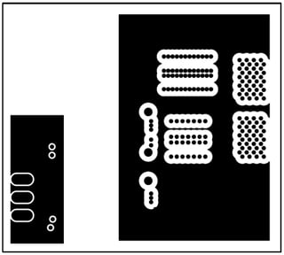
Figure 4: HEY-HBDS-G-12A1-A Top Side Copper (L) and Layer 2 Copper (R)
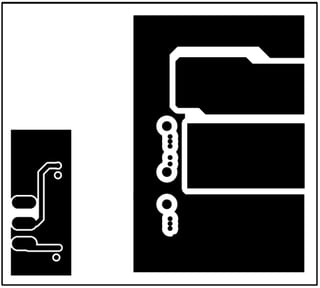
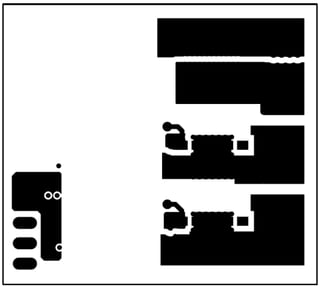
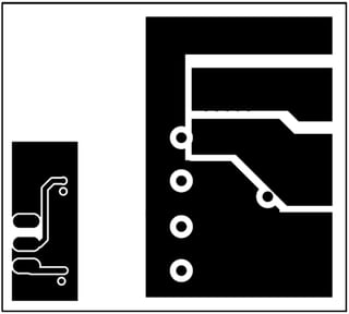
Figure 5: HEY-HBDS-G-12A1-A Layer 2 Copper(L) and Bottom Side Copper (R)
HEY-HBDS-G-12B1-A
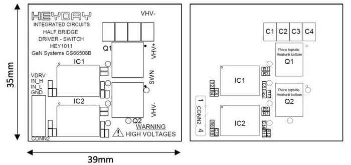
Figure 6: HEY-HBDS-G-12B1-A Silkscreen and component placement
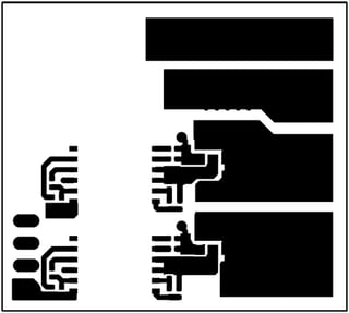
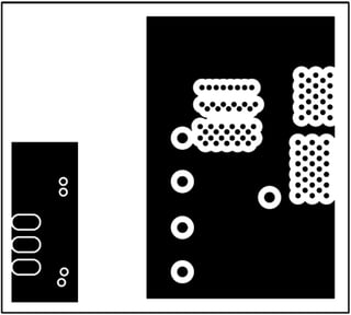
Figure 7: HEY-HBDS-G-12B1-A Top Side Copper (L) and Layer 2 Copper (R)
 .
. 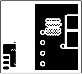
Figure 8: HEY-HBDS-G-12B1-A Layer 2 Copper(L) and Bottom Side Copper (R)
Double Pulse Test
Theory
The double pulse test is used to evaluate the switching characteristics of a power switch under hard switching but in a safe manner.
For a low side switch the set up is as shown below:
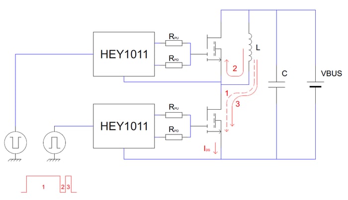
Figure 10: Double Pulse Test
The low side switch is driven with two pulses as shown below. The high side switch can be held off or driven with the inverse of the low side gate switch (with adequate dead time).

Figure 11: Double Pulse Test Waveforms
An inductor is placed in parallel with the high side switch. The goal of this inductor is to establish the test level current in the low side switch at the end of the first on pulse (1).
The falling edge of pulse 1 is used to examine the hard turn off characteristics of the switch. The rising edge of pulse 3 is used to examine the hard turn on characteristics of the switch. By only applying these two pulses, the switches are only on for a very short time and will not over heat.
Test Results
|
|
COMPONENTS |
|
Drivers: |
Heyday HEY1011-L12A |
|
Inductor: |
Wurth 74437529203471 (470uH 5.5A) |
|
RPU: |
10W |
|
RPD: |
0W |
|
CSEC: |
22nF X7R |
|
Mode: |
2 |
|
|
TEST SET UP |
|
DC Bus Voltage: |
100V |
|
Load Current: |
3.6A |
|
TON_1: |
16μs |
|
TOFF_1: |
1μs |
|
TON_2: |
1μs |
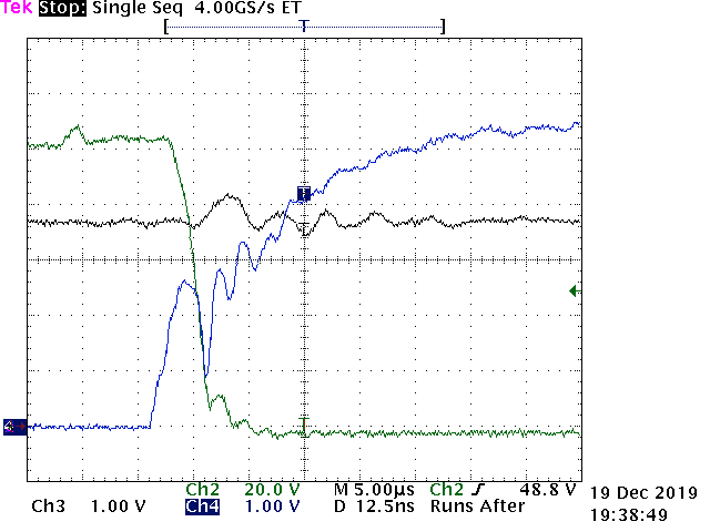
Double Pulse Overview: 100V 3.8A
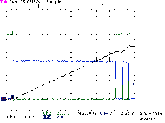
CH2(Grn): Switch Node
CH3(Blk): Inductor current (1A/V)
CH4(Blu): Low side VGS
Hard switch off: 100V 3.8A
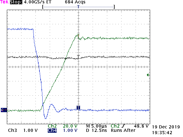
CH2(Grn): Switch Node
CH3(Blk): Inductor current (1A/V)
CH4(Blu): Low side VGS
Hard switch on: 100V 3.8A
CH2(Grn): Switch Node
CH3(Blk): Inductor current (1A/V)
CH4(Blu): Low side VGS