


71 min read

AHV85000 + AHV85040

GaN FET Isolated Gate Driver Chipset with Power-Thru Integrated Isolated Bias Supply
FEATURES AND BENEFITS
- Chipset transmits both PWM signal & bias power through a single external isolation transformer
- 50 ns propagation delay (with recommended transformers)
- Separate drive output pins: pull-up (2.8 Ω) and pull-down (1.0 Ω)
- Supply voltage 7 V < VDRV < 13.2 V
- Undervoltage lockout on primary VDRV and secondary VSEC
- Enable pin with fast response
- Continuous ON capability—no need to recycle IN or recharge bootstrap capacitor
- CMTI > 100 V/ns dv/dt immunity (with recommended transformers)
- Creepage distance > 4 or 8 mm (with recommended transformers)
- AC-DC and DC-DC converters: Totem-pole PFC, LLC half-/full-bridge, SR drive, multi-level converters, phase-shifted full-bridge, high-side cutoff switches
- Three-phase: Vienna rectifier, T-type inverter
- Industrial: transportation, robotics
- Grid Infrastructure: micro-inverters, solar
- No high-side bootstrap
- No external secondary-side bias supply
APPLICATIONS
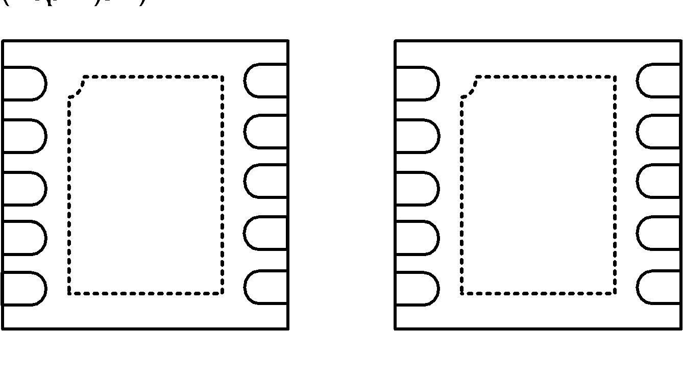
PACKAGE
DFN10 3x3 mm EJ package
DESCRIPTION
The AHV85000 & AHV85040 is a cost-optimized isolated gate drive chipset for GaN FET devices. When combined with one of the recommended external transformers, it provides a self-powered isolated gate drive solution, ideal for GaN FETs in multiple applications and topologies. A selection of recommended third-party transformers is available, each optimized for different drive voltage and gate charge characteristics, including E-mode GaN (6-V drive) and Cascode-GaN (12-V drive).
The chipset transmits both PWM signal and gate bias power through the external transformer, eliminating the need for any external gate drive auxiliary bias supply or high-side bootstrap. This greatly simplifies the system design and reduces EMI through reduced total common-mode (CM) capacitance. It also allows the driving of a floating switch in any location in a switching power topology.
The chipset enables fast propagation delay and high peak current source/sink capability to efficiently drive GaN FETs in high-frequency designs. High CMTI combined with isolated outputs for both bias power and drive make it ideal in applications requiring isolation, level-shifting, or ground separation for noise immunity.
The chipset is available in a pair of 3x3 mm DFN10 surface-mount packages. Several protection features are integrated, including undervoltage lockout on primary and secondary bias rails, internal pull-down on IN pin and OUTPD pin, and a fast-response enable input/fault-output pin.
TYPICAL APPLICATION
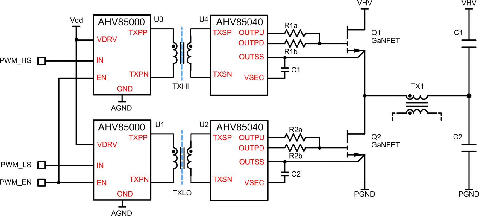
Figure 1: Typical AHV85000/040 chipset half-bridge — eliminates high-side bootstrap.
AHV85000/040-DS Advance Information Datasheet • Subject to Change Without Notice October 20, 2022
|
SELECTION GUIDE |
||||||||
|
Part Number |
IC Type |
Switch |
# of Channels |
Output |
Isolation |
Package |
||
|
AHV85000EETR |
Primary Side |
E-Mode GaN |
1 |
Unipolar |
Isolated via external transformer |
3x3 mm DFN 10-pin low-profile surface mount |
||
|
AHV85040EETR |
Secondary Side |
|||||||
ABSOLUTE MAXIMUM RATINGS (AHV85000, AHV85040)[1]
|
Characteristic |
Symbol |
Notes |
Rating |
Unit |
|
Drive Supply Voltage |
VDRV |
VDRV, wrt to GND |
VGND – 0.5 to 15 |
V |
|
Input Data |
VIN |
IN, wrt to GND |
VGND – 0.5 to 15 |
V |
|
Enable |
VEN |
EN, wrt to GND |
VGND – 0.5 to 15 |
V |
|
Select |
VSEL |
SEL to GND |
VGND – 0.5 to 15 |
V |
|
Output Drive Pull-Up |
VOUTPU |
OUTPU to OUTSS |
VOUTSS – 0.5 to 15 |
V |
|
Output Drive Pull-Down |
VOUTPD |
OUTPU to OUTSS |
VOUTSS – 0.5 to 15 |
V |
|
Isolated Bias Supply |
VSEC |
VSEC to OUTSS |
VOUTSS – 0.5 to 15 |
V |
|
Junction Temperature |
TJ |
–40 to 150 |
°C |
[1] Stresses beyond those listed under Absolute Maximum Ratings may cause permanent damage to the device. These are stress ratings only, and functional operation of the device at these or any other conditions beyond those indicated in the operational sections of the specifications is not implied. Exposure to absolute maximum rating conditions for extended periods may affect device reliability.
|
ESD RATINGS (AHV85000, AHV85040) |
||||
|
Characteristic |
Symbol |
Test Conditions |
Value |
Unit |
|
Human Body Model |
VHBM |
±2 |
kV |
|
|
Charged Device Model |
VCDM |
±500 |
V |
|
THERMAL CHARACTERISTICS: May require derating at maximum conditions; see application information
|
Characteristic |
Symbol |
Test Conditions [1] |
Value |
Unit |
|
Junction-to-Ambient Thermal Resistance |
RθJA |
Mounted on application PCB with 0.1-inch Cu heatsinking |
100 |
°C/W |
|
Junction-to-Case Thermal Resistance |
RθJC |
TBD |
°C/W |
[1] Additional thermal information available on the Allegro website.
RECOMMENDED OPERATING CONDITIONS: Valid at –40°C < TJ < 125°C, 10.5 V < VDRV < 13.2 V, CSEC = 22 nF, COUT = 1 nF,
unless otherwise stated
|
Characteristics |
Symbol |
Test Conditions |
Min. |
Typ. |
Max. |
Unit |
|
SUPPLY VOLTAGE PINS – AHV85000 |
||||||
|
Drive Supply Voltage |
VDRV |
7.0 |
– |
13.2 |
V |
|
|
INPUT PINS – AHV85000 |
||||||
|
Input Data |
VIN |
VGND |
– |
5 |
V |
|
|
Enable Active High |
VEN |
VGND |
– |
VDRV |
V |
|
|
Select |
VSEL |
VGND |
– |
VDRV |
V |
|
|
OUTPUT PINS – AHV85040 |
||||||
|
Output Pull-Up |
VOUTPU |
0 |
– |
13.2 |
V |
|
|
Output Pull-Down |
VOUTPD |
0 |
– |
13.2 |
V |
|
|
Isolated Supply Referenced to OUTSS |
VSEC |
0 |
– |
13.2 |
V |
|
|
Junction Temperature |
TJ |
–40 |
– |
125 |
°C |
|
|
Characteristics |
Symbol |
Test Conditions |
Min. |
Typ. |
Max. |
Unit |
|
VSEC Pin Capacitor CSEC |
CSEC |
External capacitance connected between VSEC and OUTSS pins; external COUT = 1 nF |
|
27 |
|
nF |
MSL RATING
|
Device |
MSL Rating |
Maximum Floor Life at Standard Ambient (30°C/60%RH) |
Maximum Peak Reflow Temperature |
Pre-Reflow Bake Requirement |
|
AHV85000 AHV85040 |
MSL-3 |
168 hours |
260°C |
Per JEDEC J-STD-033C |
Per JEDEC J-STD-033C, the AHV85110 devices are rated MSL3. This MSL3 rating means that once the sealed production packaging is opened, the devices must be reflowed within a “floor-life” of 168 hours (1 week) if they are stored in under standard ambient conditions (30°C and 60% relative humidity (RH)).
The peak reflow temperature should not exceed the maximum specified in MSL Rating table.
If the devices are exposed to the standard ambient for more than 168 hours, they must be baked before reflow to remove any excess moisture in the package and prevent damage during reflow soldering. The required bake times and temperatures are detailed in IPC/JEDEC standard J-STD-033C. If the devices are exposed to higher temperature and/or RH compared to the standard ambient of 30°C/60% RH, the floor-life will be shortened due to the increased rate of moisture absorption. If the actual ambient conditions exceed the standard ambient, it is recommended that parts should always be baked per IEC/JEDEC J-STD-033C before reflow as a precaution to avoid potential device damage during reflow soldering.
FUNCTIONAL BLOCK DIAGRAM
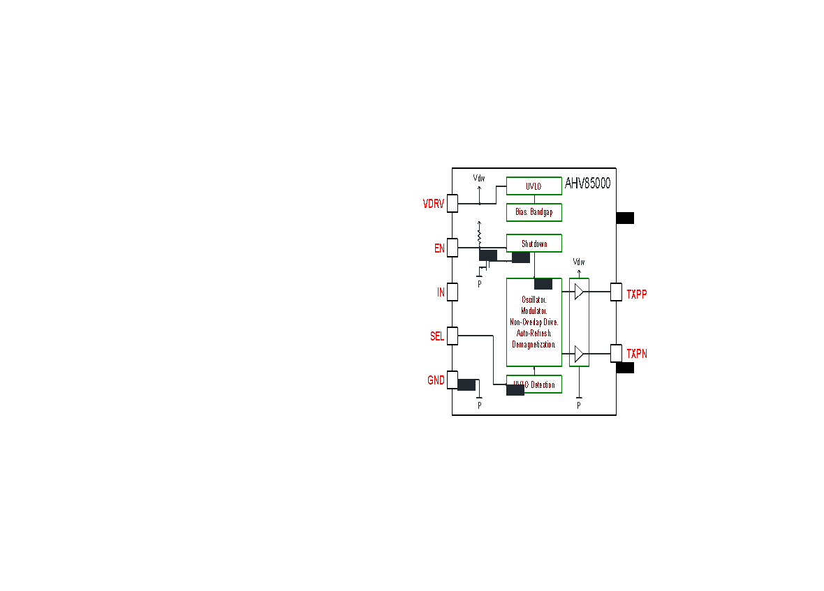
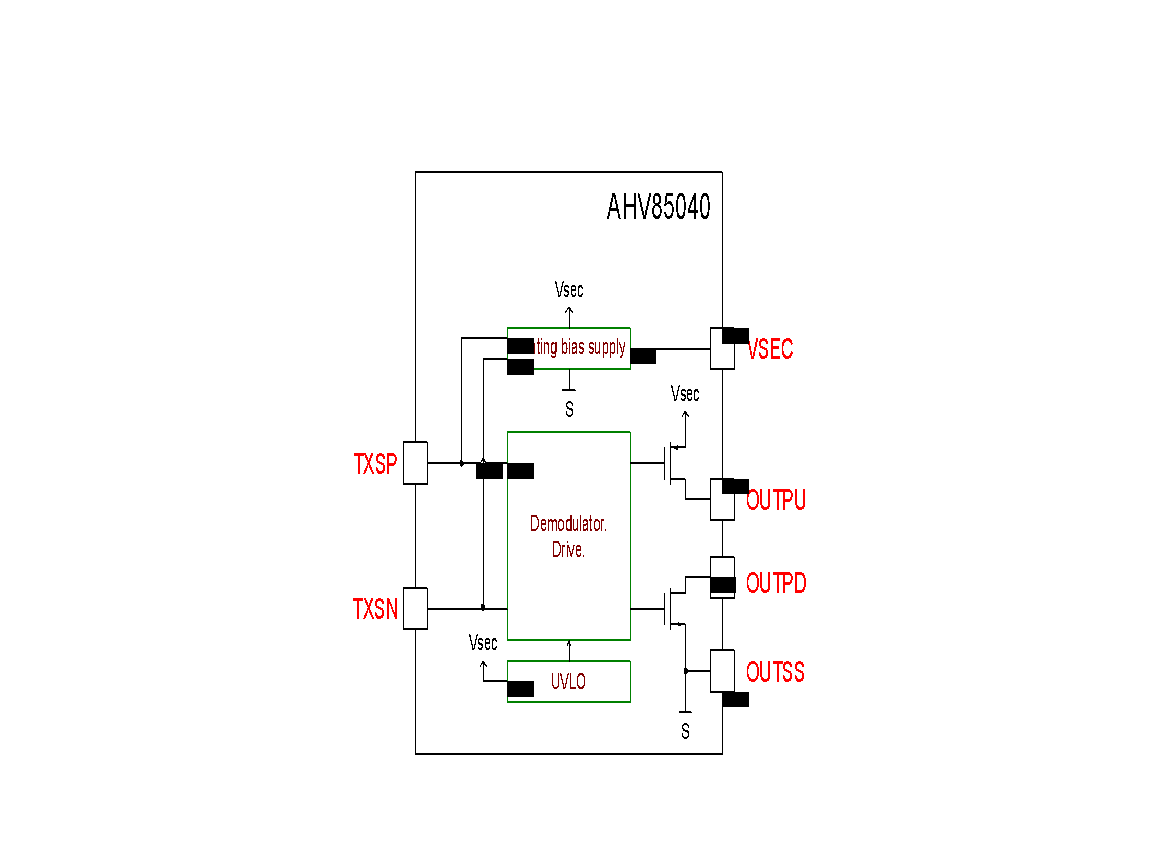
Figure 2: AHV85000 & AHV85040 Block Diagrams
PINOUT DIAGRAM AND TERMINAL LIST TABLE
Package EE Pinout
Terminal List Table
|
AHV85000 |
AHV85040 |
|||
|
Number |
Name |
Function |
Name |
Function |
|
1 |
IN |
PWM input |
NC |
No connect |
|
2 |
SEL |
UVLO select option |
OUTSS |
Secondary-side ground |
|
3 |
GND |
Primary-side ground |
TXSP |
Transformer secondary positive |
|
4 |
GND |
Primary-side ground |
TXSN |
Transformer secondary negative |
|
5 |
GND |
Primary-side ground |
OUTSS |
Secondary-side ground |
|
6 |
TXPN |
Transformer primary negative |
VSEC |
Secondary supply decoupling |
|
7 |
TXPP |
Transformer primary positive |
OUTSS |
Secondary-side ground |
|
8 |
VDRV |
Primary supply rail |
OUTPD |
Output drive pull-down |
|
9 |
GND |
Primary-side ground |
OUTPU |
Output drive pull-up |
|
10 |
EN |
Bidirectional primary-referenced enable |
OUTSS |
Secondary-side ground |
|
11 |
EP |
Exposed Pad (GND) |
EP |
Exposed Pad (GND) |
TYPICAL APPLICATIONS
Figure 3: Half-bridge with AHV85000 + AHV85040 chipset as high and low side drivers
ELECTRICAL CHARACTERISTICS: Valid at –40°C < TJ < 125°C, 7.0 V < VDRV < 13.2 V, CSEC = 22 nF, COUT = 1 nF,
unless otherwise stated
|
Characteristics |
Symbol |
Test Conditions |
Min. |
Typ. |
Max. |
Unit |
|
SUPPLY CURRENTS – AHV85000 |
||||||
|
VDRV Quiescent Current |
IDRV_DIS |
VIN = 0, VDRV = 12 V, EN = 0 |
– |
0.4 |
– |
mA |
|
VDRV Quiescent Current |
IDRV_Q |
VIN = 0, VDRV = 12 V |
– |
2 |
– |
mA |
|
VDRV Switching Current |
IDRV_SW |
fS = 100 kHz, VDRV = 12 V |
– |
4.2 |
– |
mA |
|
INPUT PINS – AHV85000 |
||||||
|
Input Data – Logic Low |
VIN(L) |
– |
– |
1.0 |
V |
|
|
Input Data – Logic High |
VIN(H) |
2.0 |
– |
– |
V |
|
|
Input Data Hysteresis |
VIN(HYS) |
– |
300 |
– |
mV |
|
|
Enable Active High – Logic Low |
VEN(L) |
– |
– |
1.0 |
V |
|
|
Enable Active High – Logic High |
VEN(H) |
2.0 |
– |
– |
V |
|
|
Enable Active High – Hysteresis |
VEN(HYS) |
– |
400 |
– |
mV |
|
|
Internal On-Chip Pull-Down Resistance On IN Pin |
RIN |
– |
300 |
– |
kΩ |
|
|
PRIMARY UNDERVOLTAGE LOCKOUT – AHV85000 |
||||||
|
VDRV UV Threshold, Rising [2] |
VDRV_UV |
SEL pin connected to VDRV |
9.5 |
10.0 |
10.5 |
V |
|
VDRV UV Hysteresis |
VDRV_UVH |
– |
0.7 |
– |
V |
|
|
VDRV UV Threshold, Rising [2] |
VDRV_UV |
SEL pin connected to GND |
6.2 |
6.6 |
6.9 |
V |
|
VDRV UV Hysteresis |
VDRV_UVH |
– |
0.4 |
– |
V |
|
|
OUTPUT PINS – AHV85040 |
||||||
|
OUTPU Pull-Up Resistance |
RPU |
– |
2.8 |
– |
Ω |
|
|
OUTPD Pull-Down Resistance |
RPD |
– |
1.0 |
– |
Ω |
|
|
High Level Source Current [1] |
ISOURCE |
VSEC = 10 V, Rext_pu = 0 Ω, COUT = 10 nF |
– |
2 |
– |
A |
|
Low Level Sink Current [1] |
ISINK |
VSEC = 10 V, Rext_pd = 0 Ω, COUT = 10 nF |
– |
4 |
– |
A |
|
SECONDARY UNDERVOLTAGE LOCKOUT – AHV85040 |
||||||
|
VSEC UV Threshold, Rising |
VSEC_UV |
3.9 |
4.3 |
4.8 |
V |
|
|
VSEC UV Hysteresis |
VSEC_UVH |
– |
0.3 |
– |
V |
|
[1] Not tested in production; guaranteed by design and bench characterization.
[2] When VDRV is below the UVLO threshold, the driver output is actively held low.
SWITCHING CHARACTERISTICS: Valid at –40°C < TJ < 125°C, 7.0 V < VDRV < 13.2 V, CSEC = 22 nF, COUT = 1 nF,
unless otherwise stated
|
Characteristics |
Symbol |
Test Conditions |
Min. |
Typ. |
Max. |
Unit |
|
PROPAGATION TIMES – AHV85000 + AHV85040 + External Transformer |
||||||
|
Propagation Delay, High To Low |
tPHL |
– |
50 |
– |
ns |
|
|
Propagation Delay, Low To High |
tPLH |
– |
50 |
– |
ns |
|
|
RISE AND FALL TIMES – AHV85000 + AHV85040 + External Transformer |
||||||
|
Rise Time |
tr |
Rext_pu = 0 Ω, 20-80% |
– |
9 |
– |
ns |
|
Fall Time |
tf |
Rext_pd = 0 Ω, 20-80% |
– |
7 |
– |
ns |
|
Shortest ON Time Allowable |
tpw(on) |
The ON time should never be less than specified minimum |
50 |
– |
– |
ns |
|
Shortest OFF Time Allowable |
tpw(off) |
The OFF time should never be less than specified minimum |
150 |
– |
– |
ns |
|
STARTUP TIME – AHV85000 + AHV85040 + External Transformer |
||||||
|
Wait Time Before First IN Edge is Delivered After VDRV is Within Specification |
tSTART |
– |
– |
500 |
µs |
|
VSEC PIN CAPACITOR
|
Characteristic |
Symbol |
Test Conditions |
Min. |
Typ. |
Max. |
Unit |
|
VSEC Pin Capacitor CSEC |
CSEC |
External capacitance connected between VSEC and OUTSS pins; external COUT = 1 nF |
10 [1] |
27 |
100 [2] |
nF |
[1] Smaller CSEC values than the recommended typical value can give higher voltage ripple on CSEC. Recommended CSEC value is 10-20 times larger than the effective load capacitance COUT
[2] Larger CSEC values will mean longer startup times.
FUNCTIONAL DESCRIPTION
The AHV85000/AHV85040 is a is a self-powered isolated gate driver chipset leveraging Allegro’s patented Power-Thru technology. The technology allows the transfer of both PWM signal and gate power across a single transformer-based isolation barrier. This eliminates the need to provide an isolated bias supply to power the isolated side of the driver, greatly simplifying the system design. Only an external decoupling capacitor is required on the isolated side. The chipset has been optimized for driving the gate of typical Schottky-gate Enhancement-mode (E-mode) GaN FETs, such as those available from GaN Systems, Innoscience, ST, Nexperia, GaN Power International, Taiwan Semiconductor, Rohm and others. In addition, some Transphorm cascode-GaN devices can also be driven, where low-voltage logic-level MOS devices are used inside the cascode. An online FET selection tool can be downloaded from the Allegro website to assist system designers, to check compatibility of various FET devices with the driver. The maximum drive capability is 30 nC at 6 V VGS. The isolated VSEC bias rail on the secondary is derived open-loop from the primary 12 V supply VDRV. The VSEC rail level regulates quite well versus PWM switching frequency FSW at the IN pin, for a given fixed VDRV level, and for a fixed load COUT at the OUTx drive pins (the load presented by the gate of the GaN FET being driven). This is because the charge delivered per PWM cycle naturally increases in tandem with the charge consumed by the FET gate, so there is a good charge balance across a wide frequency range. However, the VSEC rail does vary with effective loading of the gate of FET being driven; as VSEC level falls, more charge is available to be delivered to the secondary side, while the charge consumed by the FET gate decreases with falling VSEC level. Therefore, the VSEC rail will droop as far as needed until the charge delivered matches the charge consumed. For this reason, it’s also very important to minimize the amount of charge diverted into any external loads. For example, a very low bias power external circuit can be powered using VSEC, but the consumption should be minimal, to minimize the charge diverted away from the gate of FET. Similarly, if a gate-source pull-down resistor is desired on the load FET (to prevent false turn-on in the case of a manufacturing fault, such as an open-circuit gate turnon resistor), the resistor value should be as large as possible. The recommended value is 100 kΩ, to minimize DC loading on VSEC. Since DC load current converts to equivalent charge as Q = I × t, DC loading effects will become significantly more pronounced at lower PWM frequency, as the time duration t gets longer. Since there is just a single magnetic isolation barrier to transfer both PWM signal and gate power, this also greatly reduces the total parasitic capacitance between the primary-side and isolatedside, to typically < 1 pF total for both signal and power channels. This is much less than the typical total parasitic capacitance value for a solution using a conventional isolated gate driver with a separate isolated DC-DC bias supply, where the capacitance contribution from the DC-DC isolation transformer could be as high as 10 pF or more. This reduction in isolation capacitance greatly reduces the level of noise injected back into the low-voltage control circuit by the high-voltage and high dv/dt switching nodes in the power stage half-bridge legs, reduces system level Common-Mode (CM) EMI, and saves on power loss that occurs through repetitive charging and discharging of this parasitic capacitance between the high bus voltage level and ground.
APPLICATIONS INFORMATION
External Transformer Details
The AHV85000 and AHV85040 chipset form the primary-side transmitter (TX) and secondary-side receiver (RX) for an isolated GaN FET gate-driver. The chipset relies on an external transformer, connected between the TX and RX ICs, to achieve the isolated transmission of both PWM signal and gate bias power to the secondary side. The required transformer consists of a simple 2-winding, 4-pin structure – a primary-referenced TX winding and a secondary-referenced RX winding.
A selection of recommended transformers is listed below, along with the manufacturer and the orderable part number. Each transformer has been designed and optimized to work with the AHV85000/AHV85040 chipset interchangeably. The desired transformer can be selected to suit system design requirements, e.g. depending on the required system creepage distance, isolation rating, and the target GaN FET drive voltage and gate charge.
Table of recommended transformers
|
Transformer Part Number |
Manufacturer |
Isolation Rating |
Turns Ratio |
Target Vsec Drive Level |
|
TBD |
Bourns |
Basic |
1:1 |
6 V |
|
TBD |
Bourns |
Reinforced |
1:1 |
6 V |
|
TBD |
Wurth |
Basic |
1:2 |
12 V |
|
TBD |
Wurth |
Reinforced |
1:2 |
12 V |
Expert designers can choose to use a custom transformer design of their own. The table below lists the acceptable ranges of the key transformer parameters that must be adhered to, to ensure compatibility with the AHV85000/AHV85040 chipset.
Table of required transformer parameters
|
Transformer Parameter |
Minimum |
Nominal |
Maximum |
|
Lmag |
5 µH |
6 µH |
7 µH |
|
Lleak |
N/A |
600 nH |
700 nH |
|
Volt-seconds |
1.5 V*µs |
2 V*µs |
3 V*µs |
|
DCR Pri |
N/A |
1 Ω |
1.2 Ω |
|
DCR Sec |
N/A |
1 Ω |
1.2 Ω |
|
Np/Ns |
N/A |
1:1 or 1:2 |
N/A |
|
Frequency |
N/A |
400 kHz |
800 kHz |
Bidirectional Enable/Disable EN Pin
EN is a bidirectional open-drain pin which requires an external resistor pull-up to the VDRV pin or a suitable logic supply > 3.3 V. The EN pin allows for management of startup and fault conditions between the PWM controller and multiple drivers, through use of a shared enable EN line. Either the PWM controller or the driver can pull the EN pin low via the EN bus, as shown in Figure 8. When the EN pin is pulled low (either externally or internally), this forces the driver into a mode where the IN pin signal is ignored, and the OUT pins are disabled and actively pulled low. When the EN pin goes high, normal driver operation is enabled.
In the event of an internal driver fault condition, such as UVLO or normal startup delay, the EN pin is actively pulled low internally by the driver. This driver pull-down can be detected by the PWM controller and used as a flag for an external fault, or to flag that the driver is ready, and PWM can commence.
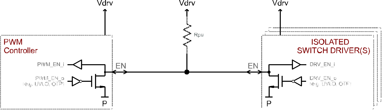
Figure 8: Example ‘Wired-AND’ connection between driver and controller
The shared EN line is typically wired-AND with the controller EN pin, as shown in Figure 8. Multiple drivers can be connected in parallel with the controller on the shared EN line, such that all connected drivers will hold the EN line low until all drivers and the PWM controller have released their own EN pin, ensuring smooth safe startup of the system.
Note that the EN pin has no internal pull-up or pull-down—the open-drain configuration relies on an external pull-up resistor for normal operation. Similarly, the EN pin must be actively pulled low externally to disable the driver. The EN pin should never
be left floating. If not used, the EN pin should be connected to VDRV through a pull-up resistor in a recommended range of 10 to 100 kΩ. The EN pin dv/dt when being pulled low or high should be at least 0.1 V/μs.
When the EN pin is pulled low, the driver output is disabled, and pulls down the OUTPD pin, regardless of the IN pin level (high or low). The driver goes to a low-power standby mode, and the isolated VSEC bias rail is allowed to discharge. The rate of decay of VSEC depends on the value of the CSEC capacitor.
When the EN pin is subsequently pulled high, the driver will re-enable, and the isolated VSEC bias rail will start to recharge.
Even if the IN pin is connected to a PWM signal, the OUT pins will not respond until the VSEC rail exceeds the secondary UVLO threshold. The rate of rise of VSEC depends on the PWM frequency at the IN pin. Worst-case slowest rise time is
when IN = 0, using the slowest internal energy-transfer mode. In this mode, the rise time will be approximately 80 μs for CSEC of 47 nF to charge from zero to the rising UVLO threshold.
Startup and Shutdown Procedures
Any PWM signal applied to IN must remain low until VDRV > UV threshold, to avoid parasitic charging of the VDRV rail
through the IN pin internal ESD structures. After VDRV exceeds the UV enable threshold, a startup time delay tSTART is required to charge VSEC and allow all internal circuits to initialize and stabilize. During tSTART, any IN signal inputs are ignored. EN internal pull-down will remain active during tSTART, and will disable (i.e., go open-drain) only when VDRV has reached its UVLO voltage level, all on-chip voltages are stabilized, and the internal tSTART timer has elapsed. Thus, the EN pin can be used via a shared EN line to flag when tSTART has elapsed, and the driver is ready to respond to PWM signals at the IN pin, as outlined above.

Figure 9: Startup relationship to be observed between VDRV, EN, and IN PWM signal.
Operating Frequency
The maximum allowable operating frequency of the AHV85000/AHV85040 chipset is dependent on the operating ambient air temperature, VDRV level, and the gate charge of the external GaNFET being driven at the OUTPU/OUTPD pins. The total power transferred from VDRV on the primary to the external GaNFET on the secondary increases with gate drive switching frequency and VDRV, hence the IC packages must dissipate more heat. The external transformer selection or custom design must be appropriate for the maximum required PWM frequency required in the system. Maximum allowable PWM frequency is 800 kHz, subject to sufficient heatsinking of the primary and secondary side ICs.
VDRV and CSEC Design Guidelines
The output gate drive amplitude is always less than VDRV. The OUTPU gate voltage level depends on factors such as VDRV level, CLOAD, and CSEC. Figure 11 shows the typical output gate drive amplitude as a function of VDRV and CLOAD, for an assumed value of CSEC as a multiple of CLOAD, for a 50% duty cycle PWM at the IN pin. This assumes a 1:1 transformer ratio setting, for the 6-V E-Mode type GaN applications.
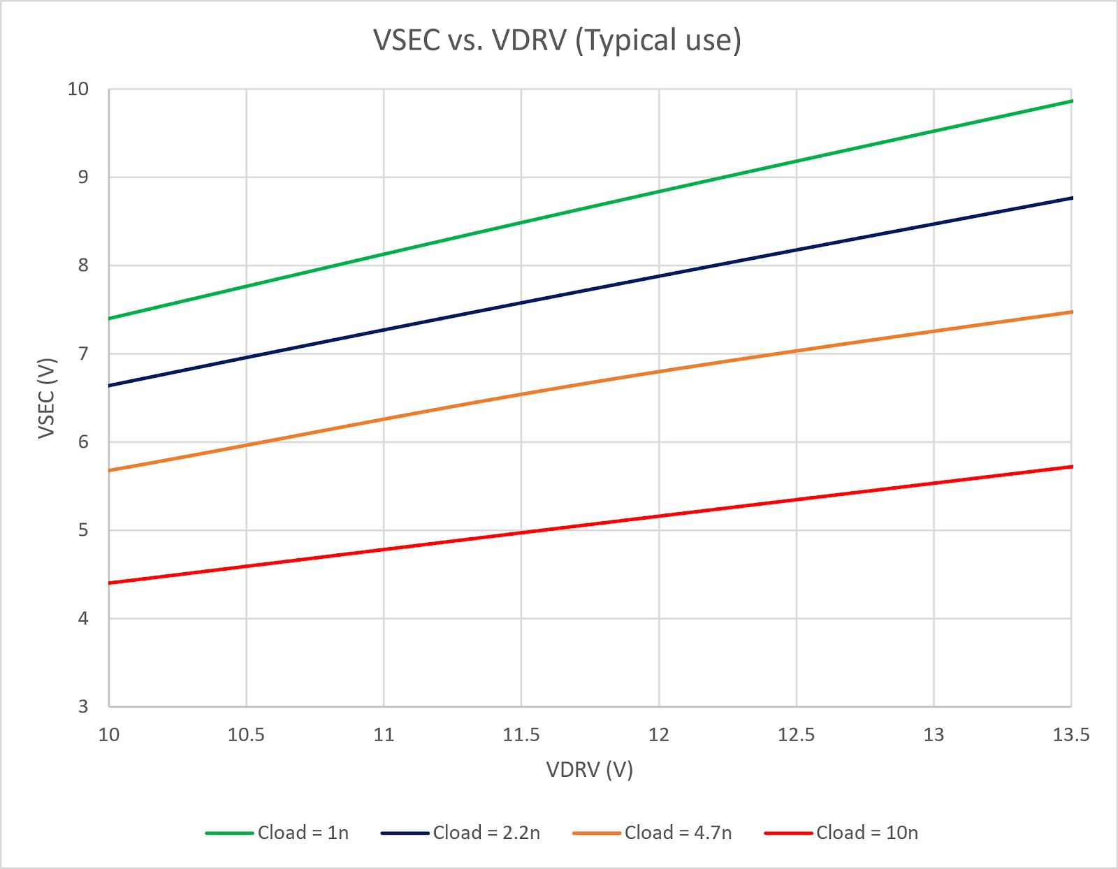
Figure 11: Typical VGATE versus VDRV for four CLOAD capacitors;
Conditions: Np/Ns 1:1, fIN = 100 kHz, D = 50%, CSEC = 20×CLOAD
The recommended value for CSEC is approximately 10 to 20 times CLOAD (the equivalent gate capacitance), to give approximately 5% to 10% switching ripple on the VSEC rail. Other values can be used; however, lower values will result is higher ripple on VSEC. Larger CSEC will require a longer startup time. The maximum recommended value of CSEC = 100 nF should not be exceeded.
Bipolar Output Drive
Bipolar output drive is used to limit the positive gate drive amplitude (relevant for E-Mode type GaN), and also provides a negative off-state gate voltage which can be beneficial in protecting against false turn on due to parasitic circuits components. It can be added simply to the AHV85040 by including three extra small external components.

Figure 12: AHV85040 bipolar output drive implementation with external Zener
PACKAGE OUTLINE DRAWING
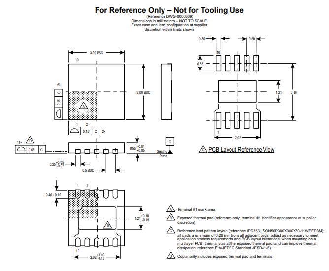
Figure 13: AHV85000 & AHV85040 EJ Package Outline and Recommended Footprint
Complete package information can be downloaded from Allegro Microsystems website: https://www.allegromicro.com/en/design-support/packaging
|
Revision History |
||
|
Number |
Date |
Description |
|
– |
October 21, 2022 |
Initial release |
|
1 |
November 17, 2022 |
Corrected Vdrv range inconsistency, corrected error in UVLO selection, updated package to EJ, updated pinouts |
Copyright 2022, Allegro MicroSystems.
Allegro MicroSystems reserves the right to make, from time to time, such departures from the detail specifications as may be required to permit improvements in the performance, reliability, or manufacturability of its products. Before placing an order, the user is cautioned to verify that the information being relied upon is current.
Allegro’s products are not to be used in any devices or systems, including but not limited to life support devices or systems, in which a failure of Allegro’s product can reasonably be expected to cause bodily harm.
The information included herein is believed to be accurate and reliable. However, Allegro MicroSystems assumes no responsibility for its use; nor for any infringement of patents or other rights of third parties which may result from its use.
Copies of this document are considered uncontrolled documents.
For the latest version of this document, visit our website:
Related Posts
Heyday Driver Architecture Enhances GaN-Based Isolated Power-Supply Designs
by CEO Joe Duigan and CTO Dr. Karl Rinne, Heyday Integrated Circuits
Allegro MicroSystems announces agreement to buy Heyday
Advanced gate driver technology significantly expands Allegro’s served addressable market in...
Meet Heyday at APEC 2022 - Attend Industry session
Heyday will be present at APEC this year again in 3 different ways:
1) We will present an...